Maker Grade vs. Research Grade EDA/GSR Sensors: Which Should You Choose?
A practical comparison of the ODAX EDA Maker and Research sensors, including their analog circuits, measurement ranges, connections, kits, and best-fit applications.
Electrodermal activity (EDA), also called galvanic skin response (GSR), is measured by applying a small excitation across two skin contacts and observing how conductance changes over time. The basic idea is simple. Building a useful sensor around it is not: electrode quality, tiny-current measurement, analog filtering, motion, ADC loading, and calibration can all affect the result.
That is why maker grade and research grade should describe the measurement workflow a sensor supports—not whether one produces “real” data and the other does not. Both ODAX boards use purpose-built analog circuitry and produce a ground-referenced analog output. The choice is mainly about how quickly you need to prototype versus how much precision, calibration detail, and measurement headroom your work requires.
Choose Maker when
You want sound relative EDA measurements, a small board, simple wiring, and a fast path through prototyping, exploration, firmware development, or an interactive build.
Choose Research when
You need a more controlled analog path, greater useful output range, calibrated conductance estimates, cross-device comparison, or data intended for deeper analysis and publication.
The circuit boards, side by side
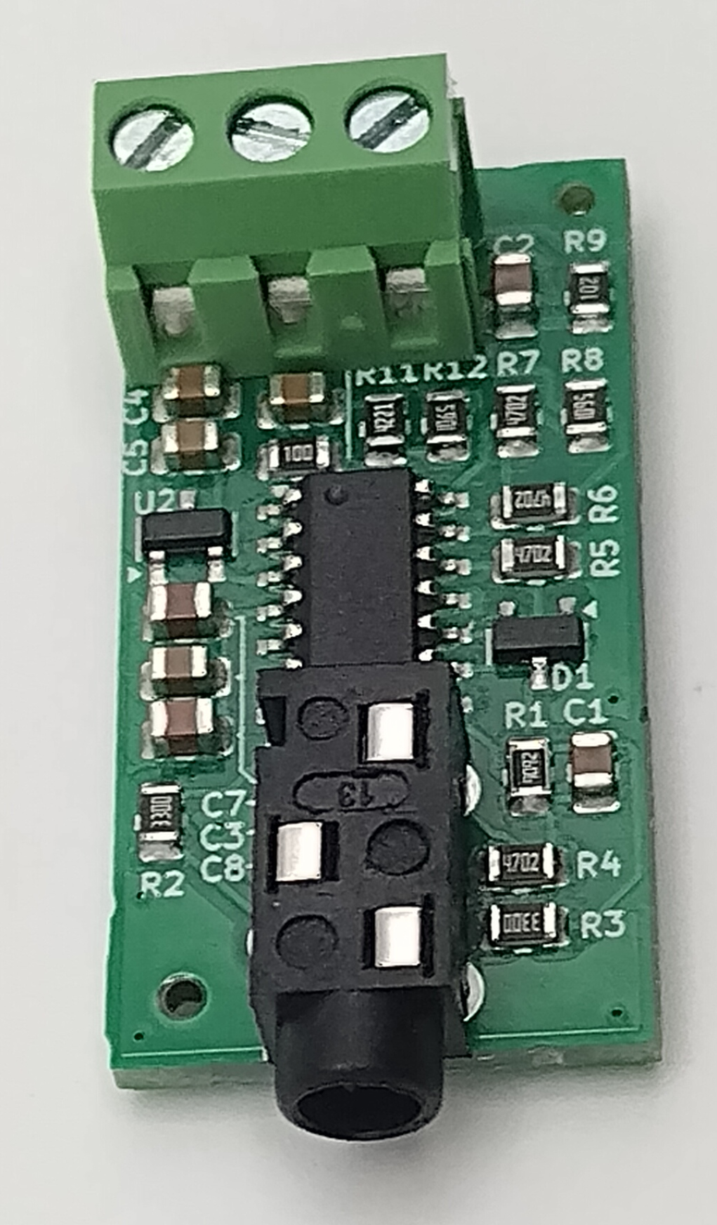
ODAX EDA Maker
33 × 17 mm compact analog board with a removable three-position terminal block.
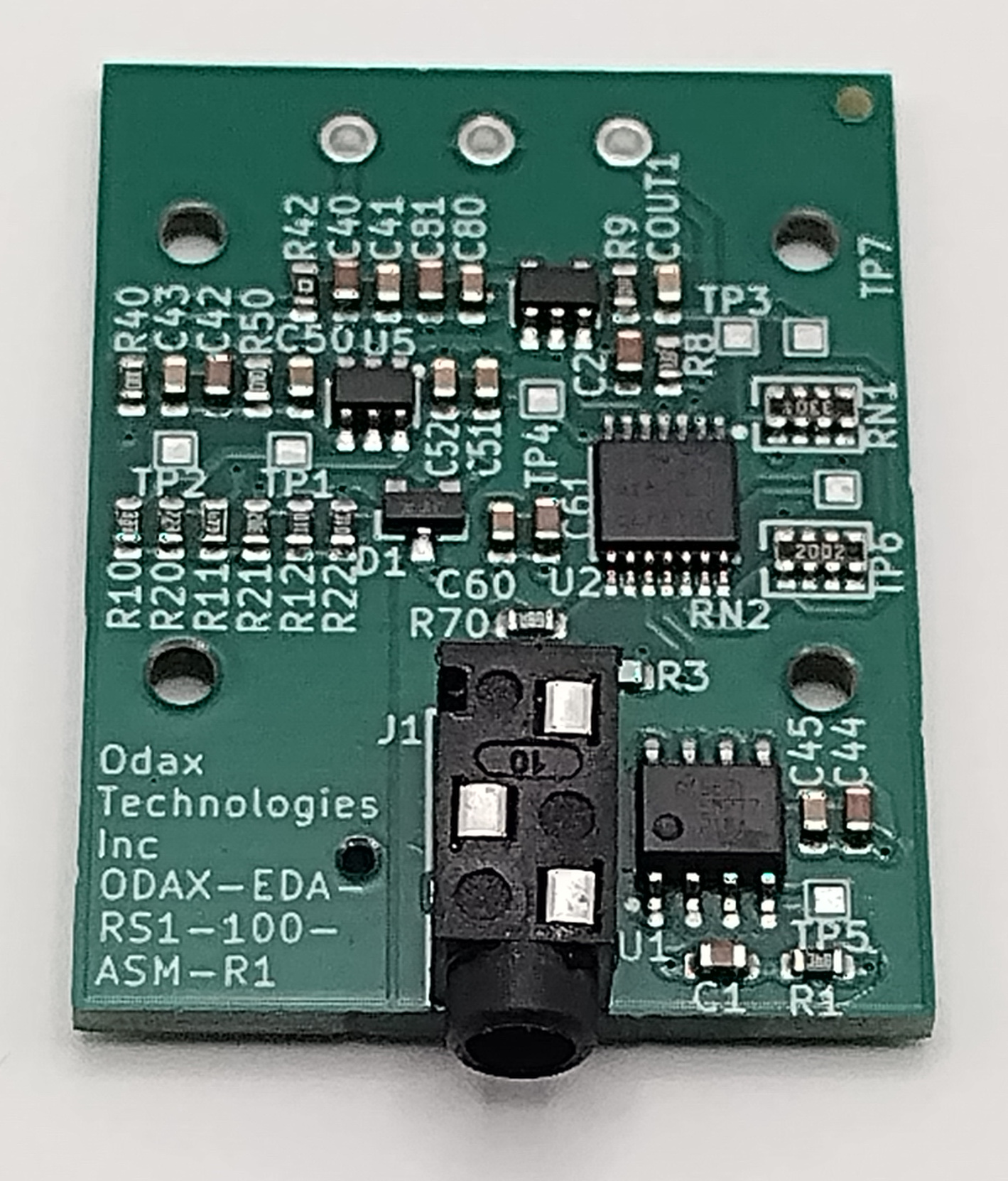
ODAX EDA Research Sensor Board
38.5 × 29 mm PCB (41 mm long with its input jack) with a guarded, low-leakage analog front end.
At-a-glance comparison
| ODAX EDA Maker | ODAX EDA Research | |
|---|---|---|
| Best fit | Prototyping, exploration, biofeedback demos, HCI, embedded development | Calibration-aware experiments, psychophysiology, DAQ systems, deeper analysis, publication-oriented work |
| Measurement architecture | All-analog, TIA-based front end with a positive-slope output | All-analog, low-leakage TIA, buffered excitation/reference, scaled subtraction, low-pass filtering, and output buffer |
| Typical use of the data | Relative trends, response timing, event detection, within-build exploration | Relative traces plus calibrated conductance estimates when measured constants and the ADC path are documented |
| Representative output / range | About 0.1–1.2 V in resistor-substitution bench observations; about 50 kΩ–1 MΩ practical simulator range | Nominal 0.135–2.5 V over 2 MΩ–70 kΩ (0.5–14.29 µS); about 70 kΩ is the near-full-scale design point |
| Useful bandwidth | DC to about 6 Hz | DC to about 6.75 Hz |
| Board-to-system connection | Screw terminal block for VIN, GND, and VOUT | Bare-board VIN, GND, and VOUT; the Research Kit exports all three on a 3.5 mm TRS cable |
| Electrode connection | 3.5 mm TS jack for two electrode contacts | Two-electrode input; the kit includes snap leads and reusable Ag/AgCl contact straps |
| Integration emphasis | Small size, easy wiring, removable terminal block | Low leakage, guarding, documented conversion model, calibration record, and enclosure options |
These ranges characterize the electronics with resistor substitution; a person is not a fixed resistor. Skin condition, hydration, electrode placement, contact pressure, motion, and cable strain can dominate the measurement in either system.
Why the Maker board goes beyond hobbyist circuitry
Some introductory GSR circuits place the skin directly in a simple resistor divider and send that node to an ADC. That can demonstrate the principle, but it leaves measurement behavior heavily dependent on the divider, the ADC, and the rest of the build.
The ODAX EDA Maker is different. It is a pure analog sensor with a TIA-based amplification and signal-conditioning path. It applies a low-voltage electrode bias, converts the resulting skin current into a positive-slope voltage, and limits the useful bandwidth to the slow range where EDA lives. Higher conductance produces higher VOUT, ready for a high-impedance microcontroller ADC.
That makes Maker a strong choice when you need good, repeatable relative measurements without first designing an analog front end yourself. It is well suited to product proofs of concept, exploratory studies, interactive systems, logging, event detection, and biofeedback work. The screw terminal provides a robust, beginner-friendly connection for VIN, GND, and VOUT; it can also be desoldered and replaced with wires or headers when a later prototype needs a different form factor.
The Maker classification is therefore about integration speed and intended measurement workflow, not a lack of real analog engineering. A careful setup can produce useful and defensible relative EDA traces. As with any sensor, validity ultimately comes from the complete protocol—not the board label alone.
What the Research board adds
The ODAX EDA Research Sensor Board is for work where small-current integrity, a controlled transfer function, and documented calibration matter more.
Its analog signal path uses a low-leakage LMP7721 transimpedance amplifier and a guarded sensitive-node layout. Buffered reference and excitation rails establish a nominal 0.5 V differential excitation. An OPA4392 stage performs scaled subtraction, an analog low-pass filter shapes the slow EDA band, and an OPA388 buffers the zero-based, ground-referenced output. In other words, it is not simply “more amplification”; it controls more of the path between the electrodes and your ADC.
The Version A output scale maps these nominal points:
| Skin resistance | Conductance | Nominal VOUT |
|---|---|---|
| 2 MΩ | 0.500 µS | 0.135 V |
| 1 MΩ | 1.000 µS | 0.264 V |
| 600 kΩ | 1.667 µS | 0.430 V |
| 220 kΩ | 4.545 µS | 1.058 V |
| 100 kΩ | 10.00 µS | 1.964 V |
| 70 kΩ | 14.29 µS | 2.500 V |
Compared with the Maker board’s representative 0.1–1.2 V output, that scaling uses more of a typical ADC input range and extends dry-range coverage to a nominal 2 MΩ. For many seated, desktop, and other indoor protocols, this provides useful detail from dry baseline through elevated conductance. Near 70 kΩ the output is already around its intended full-scale point; below that, it can clip depending on supply and ADC range.
The research datasheet also gives the resistance/conductance conversion model and lists the actual board and acquisition values to record: TIA feedback resistance, electrode-series resistance, gain, excitation and reference voltages, offsets, ADC scaling, and input impedance. That documentation is the major practical difference for teams who need reproducibility or cross-device comparison.
A note about “publication quality”
Research-grade hardware is the better starting point when values will appear in a paper, report, or deeper quantitative analysis. It does not automatically make every sample publication-quality. For calibrated absolute conductance, use measured—not merely nominal—board constants, characterize the ADC or DAQ, preserve raw samples, and report electrode placement, sampling, filtering, settling time, and artifact handling. For response timing or within-session changes, the raw voltage trace may be sufficient if the same unclipped board and acquisition path are used consistently.
The kits, side by side
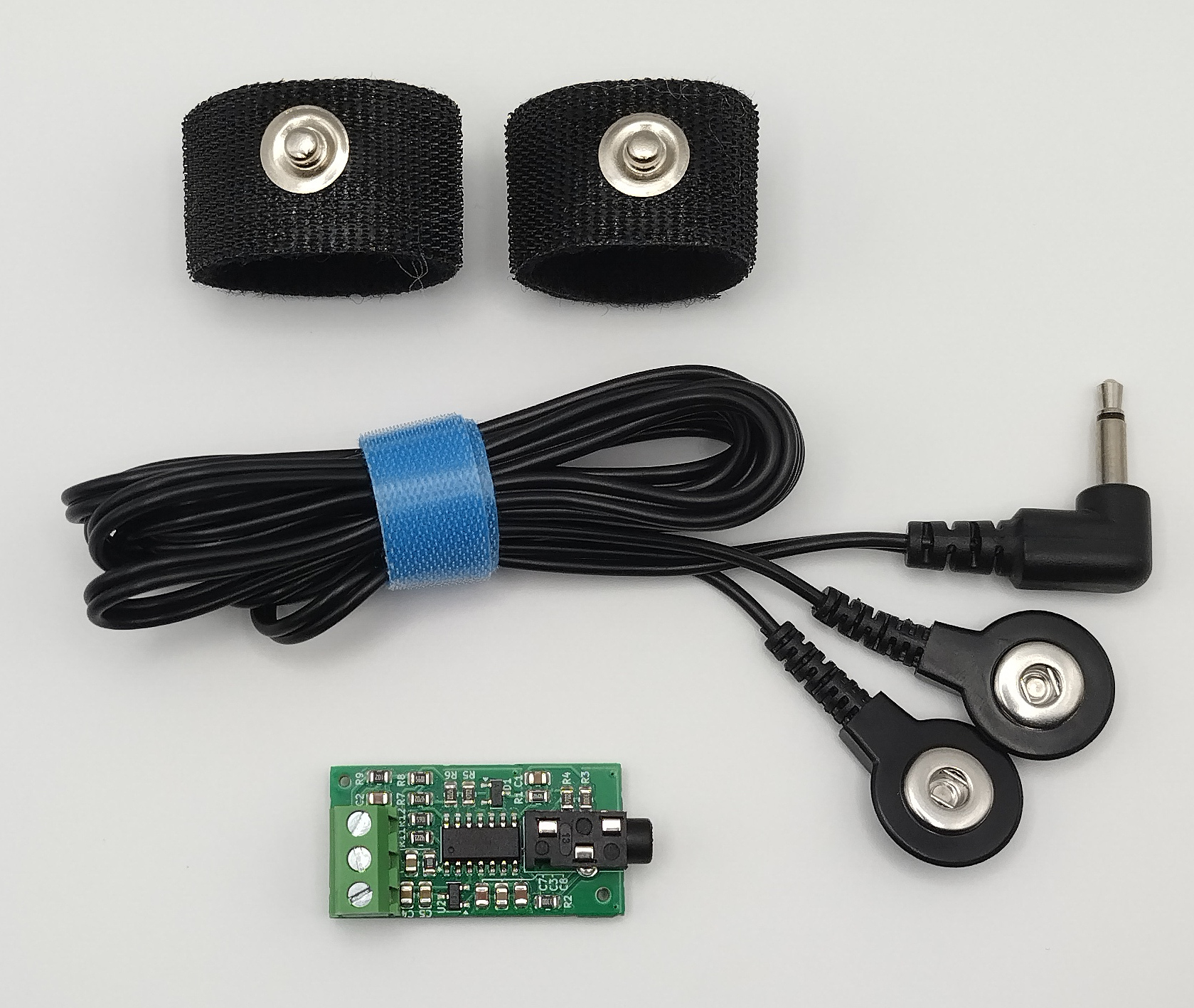
ODAX EDA Maker Kit
Maker board, reusable maker-grade black Ag/AgCl finger straps, and 3.5 mm TS electrode leads.
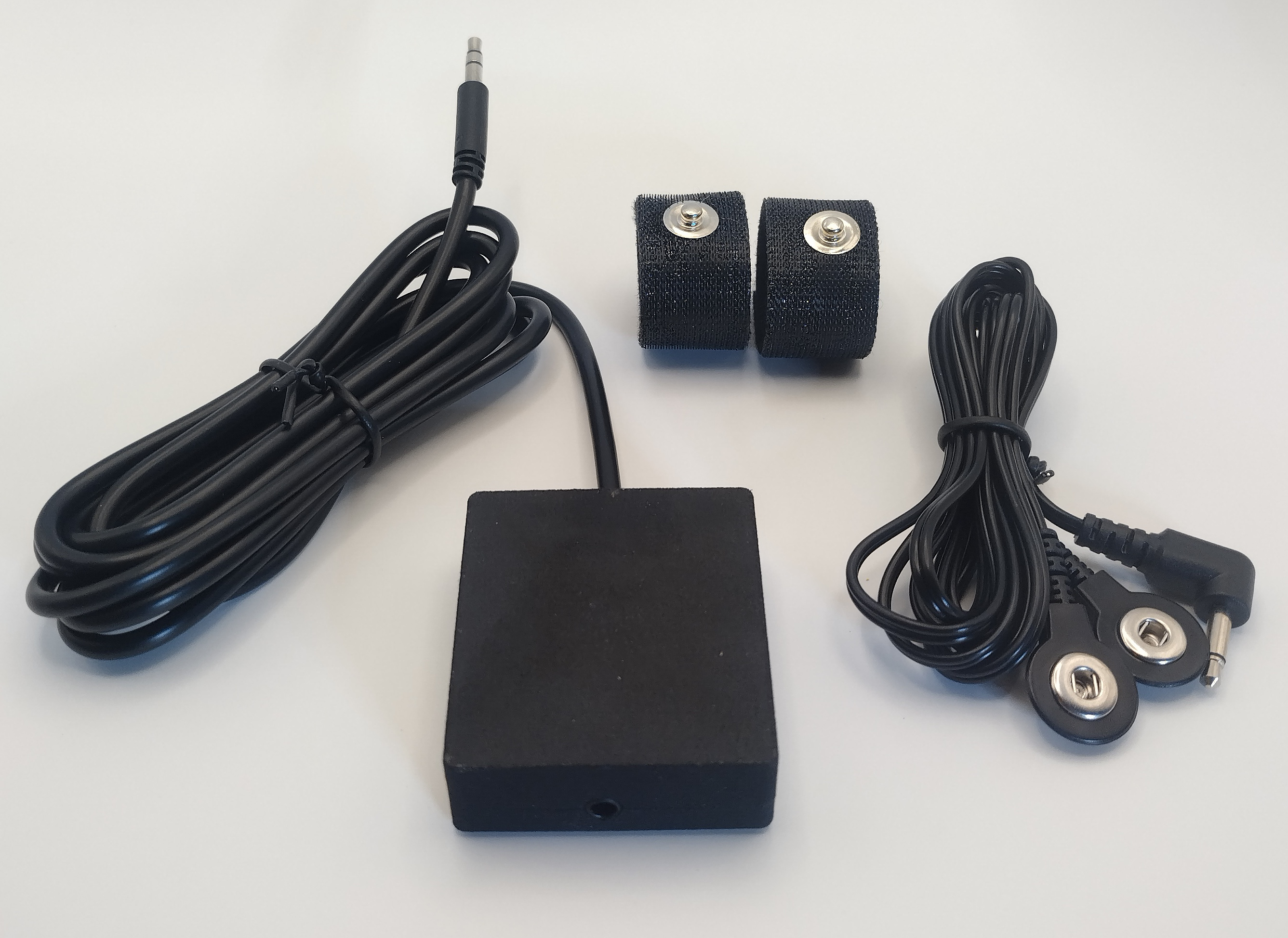
ODAX EDA Research Sensor Kit – Black
Enclosed Research board, two reusable Ag/AgCl straps, snap leads, 3.5 mm TRS sensor cable, and setup guide.
The Maker Kit is the shortest path to a working open-board prototype. Its included contacts and leads eliminate the guesswork of matching an electrode interface, while the board remains easy to wire into a breadboard or microcontroller.
The Research Kit is designed more like an instrument module. The board arrives protected inside an unmarked enclosure, and the kit includes two research-grade straps, matching snap leads, and a cable that brings the sensor output to your acquisition system.
The Research Kit’s 3.5 mm connection
The Research Kit uses the familiar 3.5 mm TRS physical standard to carry three connections on one cable:
- Tip:
VOUTsignal - Ring: 3–5 V input power (
VIN) - Sleeve: common ground (
GND)
That makes it easy to use an off-the-shelf TRS breakout or splice the cable into separate signal, power, and ground leads for a breadboard, microcontroller, custom connector, or DAQ. The plug uses an audio-style form factor, but it is not an audio connection—do not connect it to headphones or audio equipment.
The enclosure can also be opened and the Research circuit board removed for a custom wearable, benchtop housing, or other mechanical form factor. When rehousing it, preserve insulation, cable strain relief, short electrode wiring, and clearance around the guarded high-impedance input region.
Which one should you choose?
Choose the ODAX EDA Maker or Maker Kit if your immediate goal is to discover what EDA can add to a product, interaction, or experiment. It gives you robust analog sensing, simple terminal-block integration, good contacts in the kit, and enough bandwidth and range for meaningful relative measurements—without paying the integration cost of a research-focused front end.
Choose the ODAX EDA Research Sensor Board or a Research Kit in black / white when you need more precision, low-conductance detail, a documented voltage-to-conductance model, repeatable cross-system methods, or values that may be reported and published. It also fits teams who want a ready-to-use enclosure now but expect to extract the board into a custom form factor later.
In short: Maker helps you prove the idea; Research helps you characterize it. Both leave the final sampling, calibration, filtering, interpretation, and application logic in your hands.
Good measurements still depend on the whole setup
Whichever version you choose:
- Use a battery-powered or properly isolated system while electrodes contact a person; never use a mains-referenced setup without appropriate, professionally verified isolation.
- Connect
VOUTto a high-impedance ADC or DAQ input (100 kΩ minimum; higher is preferred). - Place two contacts on adjacent fingers of the same hand with comfortable, consistent pressure.
- Minimize cable movement and allow the signal to settle before baseline-sensitive analysis.
- Preserve raw samples and document filtering, scaling, electrode placement, and artifact handling.
Neither board is a medical device, and EDA is a measure of changing skin conductance—not a stand-alone diagnosis or a direct label for a particular emotion. The strongest results come from combining capable hardware with a controlled protocol and careful interpretation.