ODAX EDA Research Sensor Board
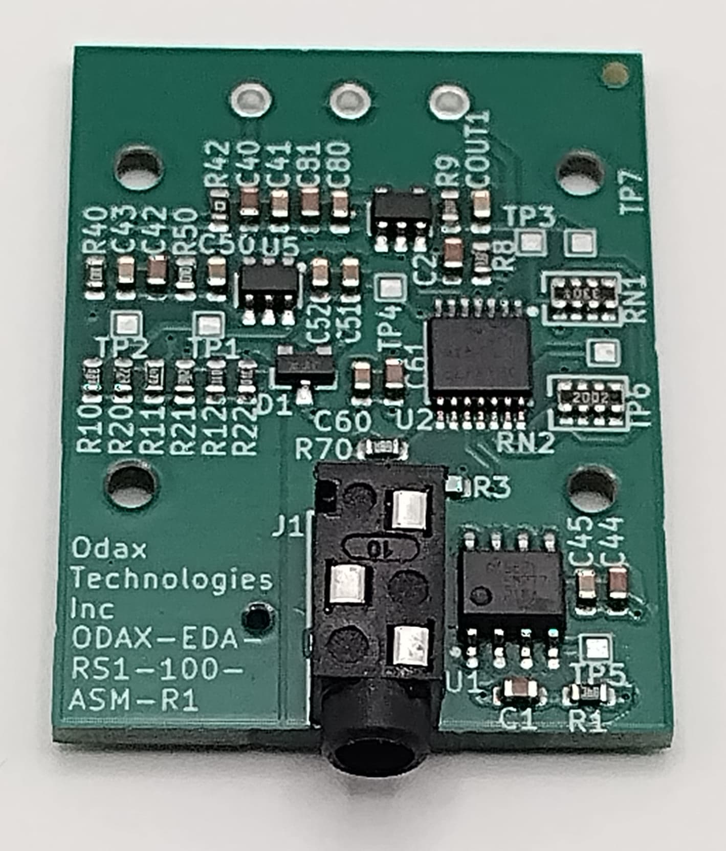
Research-grade precision electrodermal activity EDA / galvanic skin response GSR analog output sensor board for high-impedance ADC and DAQ inputs.
Overview
The ODAX EDA Research Sensor Board is a compact research-grade analog front-end board for electrodermal activity EDA (aka. galvanic skin response GSR) measurement with two skin-contact electrodes.
It is built for researchers and developers who need a stable, low-noise analog EDA/GSR signal, a documented output model, and a straightforward VOUT interface for high-impedance ADC or DAQ inputs.
At the board level, it applies a nominal 0.5 V differential excitation, measures the resulting skin-current magnitude with a low-leakage transimpedance amplifier, subtracts the buffered reference, scales the result, low-pass filters the signal, and presents a buffered zero-based analog voltage at VOUT.
The board is intended for relative EDA and GSR response timing, event-locked waveform analysis, calibrated conductance estimation, psychophysiology experiments, HCI research, biofeedback research, and custom data acquisition systems. It is not a medical device and is not intended for diagnosis, monitoring, treatment, or safety-critical use.
Why Researchers Buy It
- More precise analog front end than the maker-grade board
- Low-leakage LMP7721 TIA core for small skin-current measurements
- Guarded sensitive-node layout for improved high-impedance behavior
- Buffered reference and excitation rails for a more controlled measurement path
- Zero-based analog output that is easier to connect to an ADC or DAQ channel
- Calibration-aware output model for teams that need documented measurement constants
What You Can Build
- Research EDA and GSR acquisition systems
- Psychophysiology, HCI, affective computing, and biofeedback experiments
- Wearable or desktop sensing prototypes using two skin-contact electrodes
- Firmware, filtering, and event-detection pipelines for low-frequency conductance traces
- Custom DAQ workflows where raw analog visibility and calibration matter
Datasheet
Product Photos
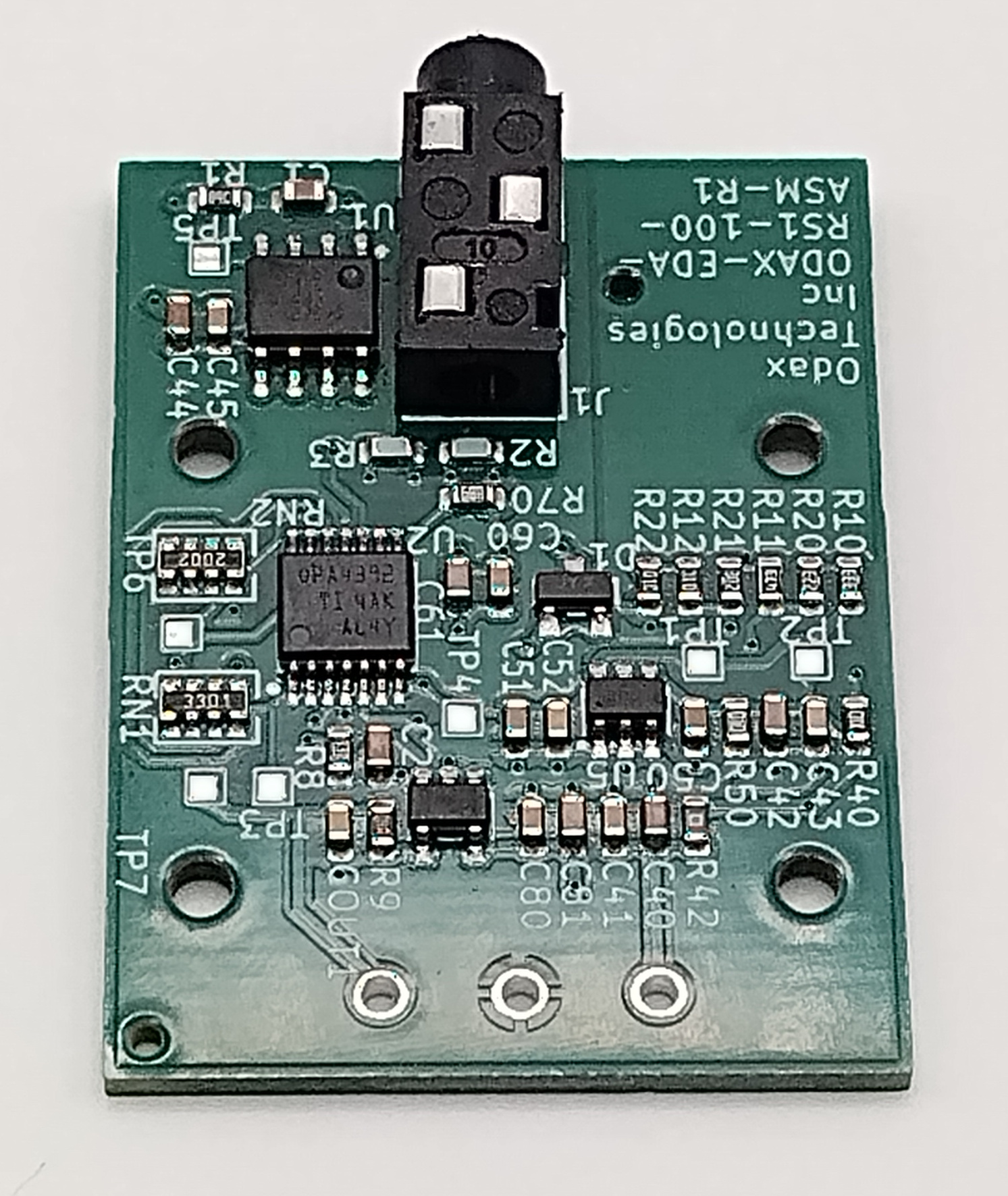
Back view
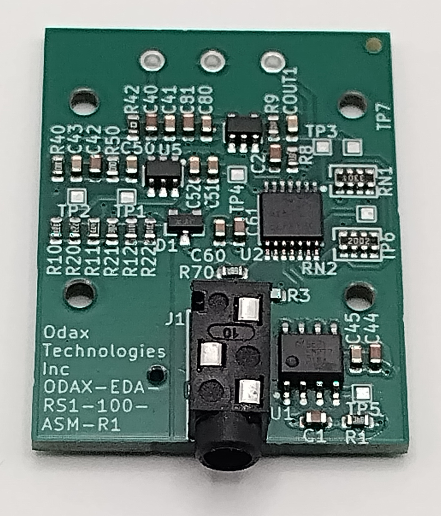
Front view
Key Features
- Research-grade EDA and GSR analog sensor board
- Low-leakage TIA core with guarded sensitive-node layout
- Nominal 0.5 V differential excitation through electrode-series resistance
- Buffered, ground-referenced
VOUTsignal for high-impedance ADC or DAQ inputs - Positive output response direction: higher conductance produces higher
VOUT - Approximate low-frequency bandwidth of 6.75 Hz for slow EDA/GSR dynamics
Built for Research Prototypes
The ODAX EDA Research Board is designed for teams that want a documented, calibration-aware analog path without designing the high-impedance front end from scratch.
For relative analysis, the voltage trace can be used directly for response timing, event-locked waveform shape, and within-session amplitude changes when the same board and ADC path are used. For calibrated conductance estimates or cross-device comparison, the datasheet documents the constants and conversion model that should be measured and recorded.
Applications
- EDA and GSR acquisition using a high-impedance ADC or DAQ input
- Psychophysiology, HCI, affective computing, and biofeedback research
- Wearable or desktop experiments using two finger straps or skin-contact electrodes
- Firmware and signal-processing development for low-frequency conductance traces
Technical Details
Recommended Operating Conditions and Electrical Characteristics
| Parameter | Symbol | Min | Typ | Max | Notes |
|---|---|---|---|---|---|
| Supply voltage, recommended | VIN | 3.0 V | 3.3 V | 5.0 V | Use a clean battery-powered or isolated low-noise supply while electrodes contact skin |
| Preferred ADC supply alignment | 3.3 V | Power from the same clean 3.3 V analog domain when practical | |||
| Reference voltage | VREF | 0.700 V | Buffered reference node | ||
| Excitation voltage | VEXC | 0.200 V | Buffered low-voltage excitation node | ||
| Excitation difference | dV | 0.500 V | Nominal differential excitation | ||
| Useful signal bandwidth | BW | DC | 6.75 Hz | Intended for slow EDA and GSR dynamics | |
| ADC input impedance | ZADC | 100 kOhm | Higher | High-impedance ADC or DAQ input preferred | |
| Output response direction | Positive | Higher conductance produces higher VOUT |
Output Scale
| Skin resistance | Conductance | Nominal VOUT | Interpretation |
|---|---|---|---|
| 2 MOhm | 0.500 uS | 0.135 V | Very dry / very low conductance |
| 1 MOhm | 1.000 uS | 0.264 V | Dry / low conductance |
| 600 kOhm | 1.667 uS | 0.430 V | Nominal expected baseline |
| 220 kOhm | 4.545 uS | 1.058 V | Moderate conductance |
| 100 kOhm | 10.00 uS | 1.964 V | Elevated conductance |
| 70 kOhm | 14.29 uS | 2.500 V | Near-full-scale design point |
User Connections
| Connection | Direction | Description |
|---|---|---|
VIN | Input | DC supply input. Recommended 3 V to 5 V from a clean battery-powered or isolated low-noise supply while electrodes contact skin |
GND | Reference | Common ground for the board and ADC or DAQ system |
VOUT | Output | Ground-referenced analog EDA/GSR output. Connect to a high-impedance ADC or DAQ input |
Mechanical
| Parameter | Nominal | Unit | Notes |
|---|---|---|---|
| PCB length | 38.5 | mm | Without input jack |
| PCB width | 29 | mm | Nominal board dimension |
| Total length | 41 | mm | With input jack |
| User electrical interface | VIN, GND, VOUT | Three simple user connections | |
| MPN | ODAX-EDA-RB1-100-ASM-R1 | Released R1 assembly |
Getting Started
- Power the board from a clean battery-powered or properly isolated 3 V to 5 V system.
- Connect
VOUTto a high-impedance ADC or DAQ input and share commonGND. - Attach two skin-contact electrodes or ODAX EDA contact straps to the electrode input.
- Place the contacts on adjacent fingers of the same hand.
- Allow the signal to settle before using the trace for baseline-sensitive analysis.
End-system performance depends on electrode condition, skin condition, contact pressure, motion, ADC scaling, ADC input impedance, firmware filtering, and calibration choices.