ODAX EDA Standard Board
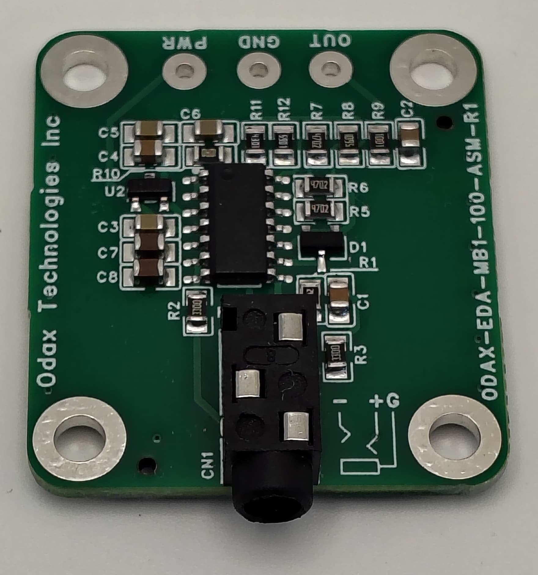
EDA/GSR analog sensor board with the ODAX EDA Maker circuit in a 35 × 31 mm form factor, four mounting holes, and PWR, GND, OUT solder connections.
Overview
The ODAX EDA Standard Board (SB1) is an assembled analog sensor board for electrodermal activity (EDA) and galvanic skin response (GSR) experiments.
It uses the same circuit and electrical routing as the ODAX EDA Maker board, part number ODAX-EDA-MB1-100-ASM-R1, in a different mechanical form factor. The Standard Board measures 35 × 31 mm and provides four corner mounting holes and three through-hole solder connections for integration into enclosures, test fixtures, and custom builds.
The board applies a low-voltage electrode bias, measures the resulting skin-current response with a transimpedance amplifier (TIA) analog front end, and provides a ground-referenced analog output for a microcontroller ADC. Higher skin conductance produces higher VOUT.
It is intended for relative EDA/GSR trend measurement, event detection, biofeedback experiments, and custom firmware development. It is not a medical device and is not intended for diagnosis, monitoring, treatment, or safety-critical use.
Why Choose the Standard Board
- The same electrical behavior as the ODAX EDA Maker board in an alternative PCB shape
- Four mounting holes for securing the board inside an enclosure or fixture
- Through-hole solder connections for suitable wires or compatible pins
- A simple analog output for your own sampling, logging, filtering, and event-detection firmware
- Compatibility with two-electrode lead setups and ODAX EDA contact straps
Datasheet
The R1 datasheet includes electrical characteristics, connection guidance, a mechanical dimension drawing, and ordering information. Its specifications are marked preliminary.
Product Photos
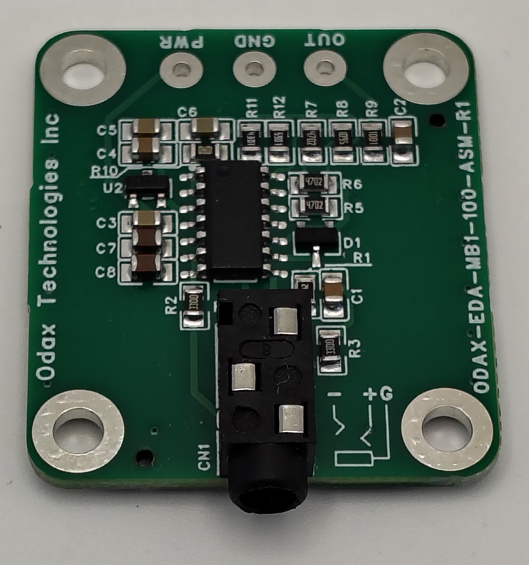
Component side with the electrode jack at the bottom
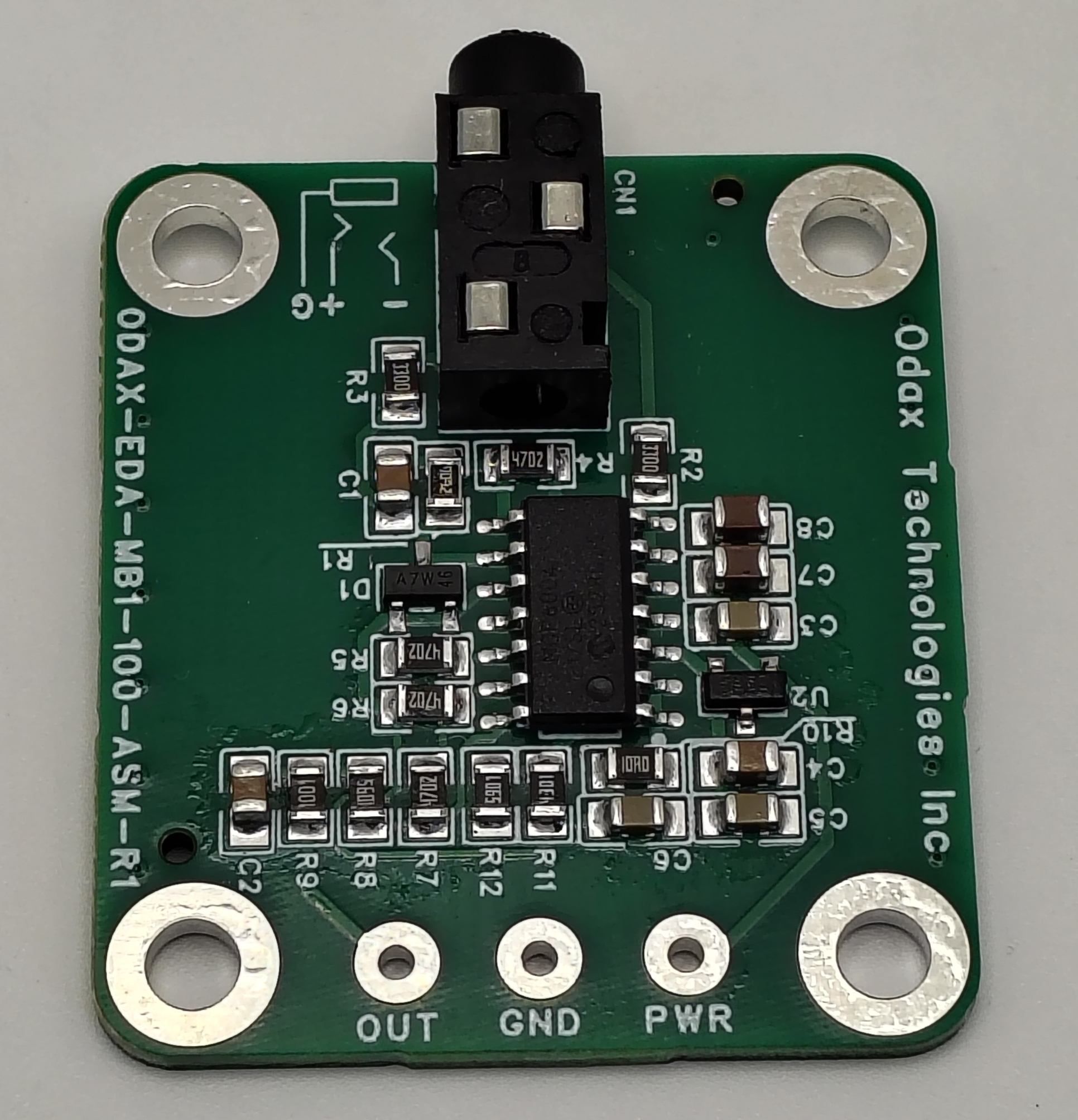
Alternate component-side view
The photographed boards retain the ODAX-EDA-MB1-100-ASM-R1 silkscreen identifier. The Standard Board SKU and MPN are ODAX-EDA-SB1-100-BLK-R1, as documented in the SB1 datasheet.
Key Features
- Maker-grade TIA-based analog EDA/GSR front end
- Positive-slope, ground-referenced output for a high-impedance ADC input
- Recommended 3 V to 5 V battery-powered operation while electrodes contact skin
- Approximately DC to 6 Hz useful signal bandwidth for slow EDA/GSR signals
- 3.5 mm TS electrode interface for two skin-contact electrodes
- 35 × 31 mm PCB with a four-hole mounting pattern
Applications
- EDA and GSR measurement for prototyping and maker projects
- Psychophysiology, HCI, affective computing, biometrics, and biofeedback experiments
- Wearable sensing prototypes using standard electrode lead sets
- Custom enclosures and acquisition systems for low-frequency analog biosignals
Technical Details
Electrical values are carried over from the ODAX EDA Maker datasheet because the circuit is unchanged. Unless otherwise stated, they are preliminary and intended for maker-level use.
Recommended Operating Conditions and Electrical Characteristics
| Parameter | Symbol | Min | Typ | Max | Notes |
|---|---|---|---|---|---|
| Supply voltage, recommended | VIN | 3.0 V | 3.3 V or 5.0 V | 5.0 V | Battery-powered system while electrodes contact skin |
| Supply voltage, tolerated functional range | VIN | 3.0 V | 5.5 V | Not the recommended operating range; verify in the end system | |
| Analog output voltage, representative use | VOUT | 0.1 V | 1.2 V | Maker-board resistor-substitution bench observations over a practical range | |
| Useful signal bandwidth | BW | DC | about 6 Hz | Intended for slow EDA/GSR signals, not high-speed biopotentials | |
| Practical resistor-simulator range | Rskin | about 50 kOhm | about 1 MOhm | Representative range; skin and electrode behavior vary | |
| ADC input impedance | ZADC | 100 kOhm | Higher impedance preferred | ||
| Output response direction | Positive | Higher conductance produces higher VOUT |
User Connections
The board labels PWR and OUT correspond to VIN and VOUT in the Maker board documentation. The electrical functions are unchanged.
| Connection | Function | Description |
|---|---|---|
PWR | VIN; input | DC supply input. Recommended 3 V to 5 V from a battery-powered system while electrodes contact skin |
GND | Reference | Common ground for the board and the ADC system |
OUT | VOUT; output | Analog EDA/GSR output. Connect to a high-impedance ADC input |
| 3.5 mm jack tip | E+ | Electrode drive contact. Connect to one skin-contact electrode or strap |
| 3.5 mm jack sleeve | E- | Measurement return contact. Connect to the second skin-contact electrode or strap |
| 3.5 mm jack ring | NC | If a TRS jack or plug is used mechanically, the ring contact is not used by the board |
With the component side facing you and the electrode jack at the bottom, the upper solder connections are PWR, GND, OUT from left to right. Verify the labels on the supplied board before wiring. Do not intentionally connect either electrode contact to GND.
The board uses through-hole solder connections without a fitted terminal block. Solder suitable wires or compatible pins as required, taking care not to damage the PCB pads or nearby components.
Mechanical
| Parameter | Nominal | Unit | Notes |
|---|---|---|---|
| PCB length | 35.0 | mm | Board outline; excludes jack projection |
| PCB width | 31.0 | mm | Board outline |
| Mounting holes | 4 | One at each corner | |
| Mounting-hole diameter | 3.2 | mm | As shown in the datasheet dimension drawing |
| Mounting-pad outside diameter | 6.2 | mm | Circular pad around each mounting hole |
| Hole spacing, along length | 28.0 | mm | Center to center |
| Hole spacing, across width | 24.0 | mm | Center to center |
| Board format | Assembled PCB | Four-hole mounting pattern | |
| Electrode connector | 3.5 mm jack | Used as TS for two electrode lead contacts | |
| User electrical interface | PWR, GND, OUT | Three through-hole solder connections |
Dimensions are nominal. PCB thickness, assembled height, connector projection, and mechanical tolerances are not specified in the supplied drawing. Allow clearance for the electrode jack and inserted plug when designing an enclosure.
Getting Started
- With power off, solder suitable wires or compatible pins to
PWR,GND, andOUT, checking the board labels before wiring. - Connect
OUTto a high-impedance ADC input and share commonGNDwith the ADC system. - Attach two skin-contact electrodes or ODAX EDA contact straps through the 3.5 mm electrode jack.
- Use a battery-powered 3 V to 5 V supply connected to
PWRandGND. - Place the contacts on adjacent fingers of the same hand, keep pressure comfortable and consistent, and route the cable to minimize motion.
Use battery power only while electrodes contact skin. Do not power the board from a mains adapter while connected to a person, or connect it to mains-referenced instruments unless the complete system has appropriate isolation designed and verified by a qualified person. Do not exceed 5.5 V on PWR or drive OUT from another source.
End-system performance depends on electrode condition, skin condition, contact pressure, motion, firmware filtering, ADC resolution, and user calibration.
Ordering Information
- Product: ODAX EDA Standard Board
- SKU / part number: ODAX-EDA-SB1-100-BLK-R1
- Manufacturer part number (MPN): ODAX-EDA-SB1-100-BLK-R1
- Product family: EDA Maker Grade Analog
- Packaging: Single assembled board
Contact straps are accessories. A typical finger EDA/GSR setup uses two straps connected to the two electrode lead contacts:
- ODAX EDA Contact Strap - Maker Grade - Black
- ODAX EDA Contact Strap - Black
- ODAX EDA Contact Strap - White
Contact us for product and ordering inquiries.