ODAX Reflective PPG Sensor
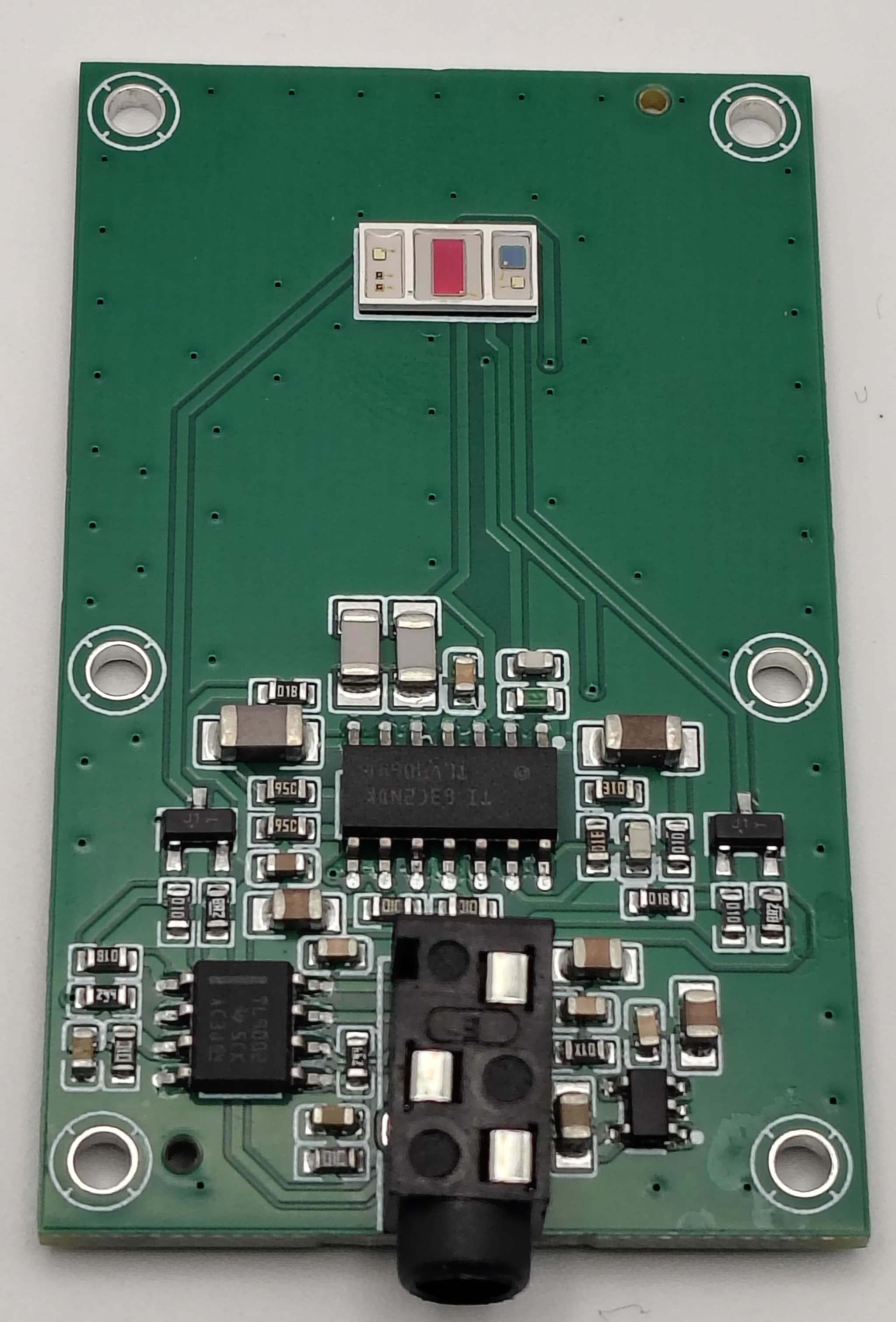
Green reflective finger PPG sensor with an ams OSRAM SFH 7072 optical module, analog signal conditioning, and a filtered voltage output for a host ADC.
Overview
The ODAX Reflective PPG Sensor is a standard-grade analog sensor board for finger photoplethysmography (PPG). It is identified as ODAX PPG Standard in the datasheet.
The board uses an ams OSRAM BIOFY SFH 7072 optical module with two green emitters and an IR-cut photodiode. The emitters and detector face the same side of the finger, measuring changes in reflected light associated with the pulse.
Its analog signal path converts photodiode current to voltage, suppresses the steady optical background, amplifies pulse variations, and filters the result. The VOUT signal connects to a high-impedance host ADC, leaving sampling, pulse detection, and rate estimation to your own firmware or software.
SKU / MPN: ODAX-PPG-SR1-100-STD-R1
Why Choose the ODAX PPG Sensor
- An assembled optical and analog front end for finger-pulse experiments
- Direct access to the analog waveform for your own acquisition and signal-processing workflows
- Two continuously driven green emitters with a nominal current setpoint of 6.10 mA each
- A regulated analog supply and buffered reference for a nominal settled output baseline of 1.25 V
- Six mounting holes for integration into fixtures and custom enclosures
Datasheet
The six-page R1 datasheet includes electrical and optical characteristics, circuit operation, representative simulations, mechanical dimensions, connection guidance, and ordering information. The document is dated 2026-10-20 and its specifications are preliminary.
Product Photos
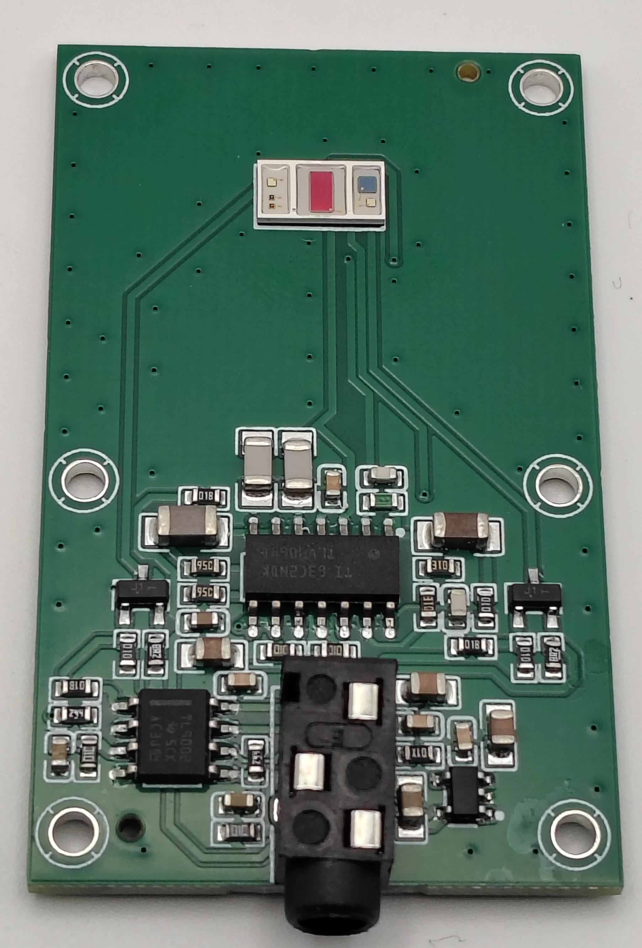
Component side with the optical sensor at the top and connector at the bottom
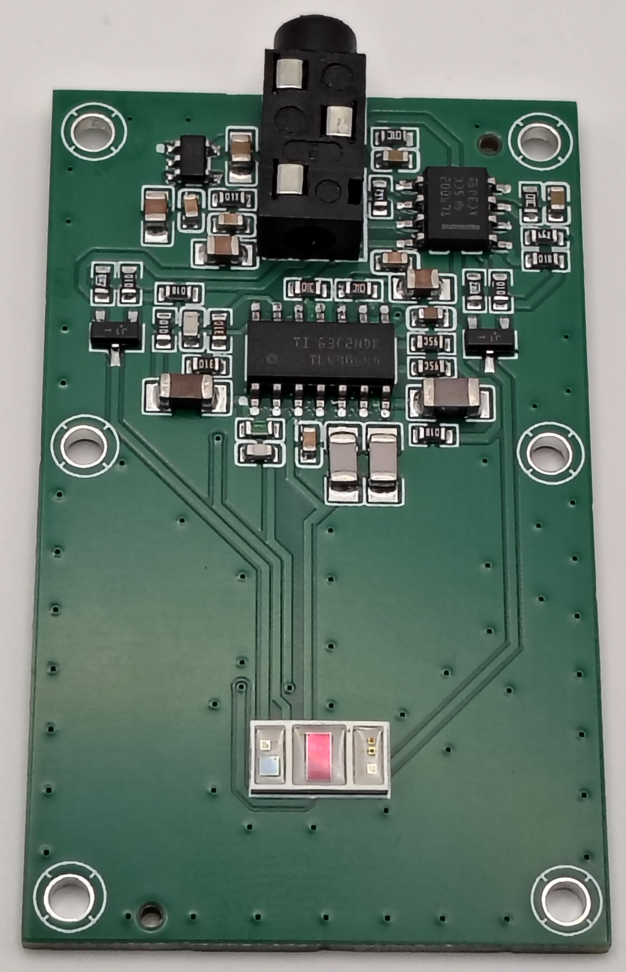
Alternate component-side view
Applications
- Reflective finger-pulse experiments
- Biofeedback prototypes
- Analog biosignal acquisition and host-side pulse-processing development
Technical Details
The values below are nominal design values from the preliminary R1 datasheet, rather than measured production limits. The board supplies an analog waveform; pulse detection and rate estimation are performed by the host.
Electrical Characteristics
| Parameter | Nominal / range | Notes |
|---|---|---|
External supply, VCC | 3.0 V to 5.0 V | Design evaluation range; use 3.3 V or 5.0 V nominal and check LED current regulation at the low end |
| Internal analog supply | 2.5 V | LP5907MFX-2.5 regulator; separate from external VCC |
| Buffered reference | 1.25 V | Nominal settled output baseline |
| Green LED drive | 6.10 mA per emitter | Calculated setpoint for each of two continuously driven emitters, subject to sufficient driver headroom |
| Total board current | Not characterized | The two LED branches alone contribute approximately 12.2 mA |
| TIA transimpedance | 47 kOhm | Photodiode current-to-voltage conversion |
| AC-stage gain | 20 V/V | Nominal midband gain magnitude, approximately 26 dB |
| High-pass corner | 0.159 Hz | Nominal first-order corner of the AC-coupled gain stage |
| Gain-stage upper pole | 36.2 Hz | Additional first-order low-pass response |
| Active low-pass filter natural frequency | 19.4 Hz | Second-order stage; not the overall -3 dB bandwidth or a guaranteed pulse-rate limit |
Output, VOUT | Analog, DC-biased | Centered near 1.25 V after settling; swing is limited by the 2.5 V analog supply and amplifier headroom |
| Output series resistance | 1 kOhm | Followed by 10 nF to ground; use a high-impedance ADC input |
Optical Configuration
The SFH 7072 is used with its two green LEDs and IR-cut detector. The green centroid wavelength is typically 530 nm at the component manufacturer's 20 mA, 25 °C test condition; this board uses the lower LED drive current listed above.
The module's red and infrared emitters and broadband detector are unused in this implementation. The board does not provide an SpO2 output.
User Connections
The datasheet identifies the connections by CN1 (PJ-3200) terminal number:
| CN1 terminal | Signal | Direction | Connection |
|---|---|---|---|
| 2 | VCC | Input | External DC supply |
| 3 | GND | Reference | Common return for the supply and host ADC |
| 4 | VOUT | Output | Filtered analog PPG voltage to the host ADC |
Verify the plug tip/ring/sleeve mapping on the actual cable before applying power. The connector carries sensor power and signal and must not be connected to audio equipment.
Mechanical
| Parameter | Nominal | Unit | Notes |
|---|---|---|---|
| PCB length | 52.5 | mm | Board outline |
| PCB width | 32.0 | mm | Board outline |
| PCB thickness | 1.6 | mm | Nominal board thickness |
| Mounting holes | 6 | Mounting-hole pads connect to GND | |
| Mounting-hole diameter | 2.2 | mm | Verify the delivered board before making close-fitting mounting hardware |
| Outer hole spacing | 47.0 × 27.0 | mm | Nominal mounting pattern |
| Middle to end column | 20.5 | mm | Nominal mounting-hole column spacing |
| Height to top of connector | 6.6 | mm | Measured from the PCB underside |
Dimensions are nominal and do not specify manufacturing tolerances. Allow clearance for soldered pins beneath the PCB and for the plug beyond the board edge. Keep the optical face unobstructed, provide gentle and stable finger contact, and add cable strain relief to limit motion. Account for the grounded mounting-hole pads when selecting conductive fasteners or an enclosure.
Getting Started
- With power off, verify the cable connections to
VCC,GND, andVOUT. ConnectVOUTto a high-impedance host ADC and share the signal ground. - Apply a clean supply within the 3.0 V to 5.0 V design range. Use 3.3 V or 5.0 V nominal as a starting point, and keep
VOUTwithin the ADC's permitted input range. The board's analog domain remains 2.5 V even whenVCCis 5 V. - Rest the finger pad over the optical package with light, consistent pressure. Shield it from strong ambient light and support the hand and cable.
- Allow several seconds for the baseline to settle after power-up or repositioning, and discard that settling interval.
- Start acquisition at 100–200 samples per second. Inspect the waveform for clipping, motion, and baseline drift before selecting filtering and peak-detection settings.
- Estimate pulse rate from accepted pulse intervals: divide 60 by the interval in seconds to obtain beats per minute. Reject corrupted intervals and validate the algorithm for its intended use.
Interpreting the Signal
Pulse amplitude depends on finger placement, contact pressure, tissue properties, ambient light, and motion. The high-pass stage suppresses steady background in the downstream signal, but cannot recover a saturated photodiode front end. Motion that overlaps the pulse frequencies can remain after filtering.
The datasheet does not specify board-level pulse-rate accuracy, noise floor, temperature range, absolute maximum ratings, or medical diagnostic performance. Its simulated voltage spans and nominal frequency calculations are not guaranteed operating limits.
Ordering Information
- Product: ODAX Reflective PPG Sensor
- Datasheet product name: ODAX PPG Standard
- SKU / manufacturer part number (MPN): ODAX-PPG-SR1-100-STD-R1
- Product family: PPG Standard Grade Analog
- Format: Assembled green reflective PPG sensor board with analog output
- Revision: R1
Contact us for product and ordering inquiries.